| 品牌:MAP |
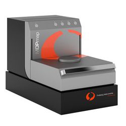
MDPmap is designed as a compact bench top contactless electrical characterisation tool for offline production control or R&D, measuring parameters like carrier lifetime, photoconductivity, resistivity and defect information over a wide injection range in steady state or short pulse excitation (μ-PCD). Automated sample recognition and parameter setup allows an easy adaption to a big variety of different samples comprising epitaxial layers, after various preparation stages ranging from as-grown wafers to up to 95% metallised ones. MDPmap设计为紧凑型台式非接触式电气表征工具,用于离线生产控制或研发,在稳态或短脉冲激励(μ-PCD)下在宽广的注入范围内测量载流子寿命,光电导率,电阻率和缺陷信息等参数。自动样品识别和参数设置允许在从生长晶圆到高达95%金属化晶圆的各种准备阶段之后轻松适应各种不同的包括外延层的样品。 The major advantage of MDPmap is its high flexibility. Which allows for instance the integration of up to four lasers either for injection level dependent lifetime measurements ranging from ultra low to high injection or extracting depth information by using different laser wavelengths. Bias light facility is included as well as options for μ-PCD or steady state injection conditions. A customer defined calculation with different maps is possible as well as an export of primary data for further evaluation. For standard metrology tasks a predefined standard enables routine measurements by only pushing one button. MDPmap的主要优点是其高度的灵活性。其允许例如集成多达四个激光器用于从***注入到高注入的注入水平相关寿命测量或通过使用不同的激光波长提取深度信息。包括偏压照明设施以及μ-PCD或稳态注射条件的选项。客户可以使用不同的地图进行计算,也可以导出主要数据以供进一步评估。对于标准的计量任务,预定义的标准只需按一个按钮即可进行常规测量。 Advantages Topographic visualisation of electrically active defects or material properties at almost any production stage, allows for process optimisation and performance prediction of devices. Extremely versatile measurement strategies allow special investigations as well as traceability to international standards. Small compact bench top tool with very high measurement sensitivity facilitates fast routine measurements 优点 几乎任何生产阶段的电活性缺陷或材料属性的拓扑可视化允许对器件进行工艺优化和性能预测。 非常通用的测量策略允许进行特殊调查以及追溯到***。 具有极高测量灵敏度的紧凑型小型台式工具有助于快速进行常规测量