| 品牌:MAP |
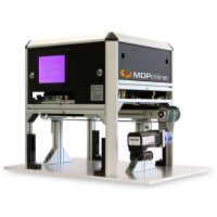
The MDPinline is Production integrated high speed wafer mapping of carrier lifetime. Single wafer topograms in less than one second a wafer. MDPinline生产集成高速晶圆映射的载体。单一晶片topograms晶片,在不到一秒的时间。 The MDPinline is a compact high speed production integrated mapping tool for quantitative measurements of carrier lifetime. Topograms are measured ‘on the fly’ in less than a second a wafer while the wafers are moved underneath the instrument by the conveyor as installed in the factory. MDPinline是一个紧凑的高速生产集成映射工具载体寿命的定量测量。Topograms测量“动态”在不到一秒的晶片,晶片由输送机移动在仪器安装在工厂。 The MDPinline itself uses no mechanically moving parts making it extremely reliable also under continuous operation. The availability of a full topogram for each individual wafer offers new ways to increase the cost effectiveness and efficiency of production lines which were so far completely out of scope. For example, an automated statistical evaluation of 10.000 wafer topograms, which are obtained within less than three hours, reveal surprisingly fine details of the performance of crystal growth furnaces as well as material quality. Processing steps such as diffusion and passivation may be ramped up and optimised within so far impossible timescales at highest performance, due to real time quality and homogeneity investigation. In the running production, any failure of a processing step may be detected immediately. On the other hand, if wafers are sold to a customer, higher prices are achieved, if each wafer exhibits a guaranteed performance leading to a return of investment for the MDPinline within less than a year. MDPinline本身不使用机械移动部件,因此在连续运行时也非常可靠。为每个晶圆提供完整的topogram提供了新方法来提高目前完全超出范围的生产线的成本效益和效率。例如,在不到三小时的时间内获得的10.000片晶格的自动统计评估揭示了晶体生长炉的性能以及材料质量的令人惊讶的细节。由于实时质量和均匀性调查,处理步骤(如扩散和钝化)可能会在性能的极不可能的时间尺度内得到加强和优化。在正在运行的生产中,可能会立即检测到任何处理步骤的失败。另一方面,如果晶片是卖给客户,实现更高的价格,如果每个晶片表现出***的性能,导致投资的MDPinline在不到一年的时间获得回报。 Advantages Full electrical wafer characterisation at speeds up to one wafer in less than a second. Measured parameters: Carrier lifetime (full topogram), resistivity (two line scans). So far not seen efficiency of process control, yield and process improvement allow for an extremely fast upramping of new fabs or processes, since statistical information from thousands of wafers are obtained in a very short period of time.Suitable for measurement of material quality of outgoing or incoming wafers as well as identification of crystallisation problems at wafer level for instance in PV industry. Well suited for diffusion process integrity control, passivation efficiency and homogeneity control. 优点 全速电子晶圆表征的速度不到一秒钟即可达到一个晶圆。测量参数:载流子寿命(全部天文图),电阻率(两行扫描)。 迄今为止,没有看到过程控制,产量和工艺改进的效率,因为可以在极短的时间内获得数千个晶圆的统计信息,因此可以***提升新的晶圆厂或工艺的速度。 适用于测量输出或输入晶圆的材料质量,以及确定晶圆级别的结晶问题,例如光伏行业。非常适合扩散工艺完整性控制,钝化效率和均匀性控制。